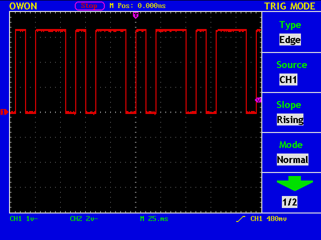
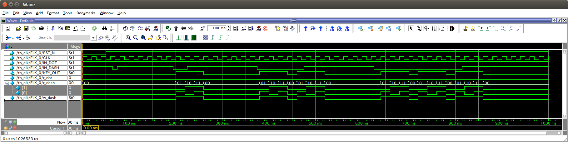
The waveform of the KEY output signal from the FPGA board while squeezing.

Ham Radio Blog
The waveform of the KEY output signal from the FPGA board while squeezing.
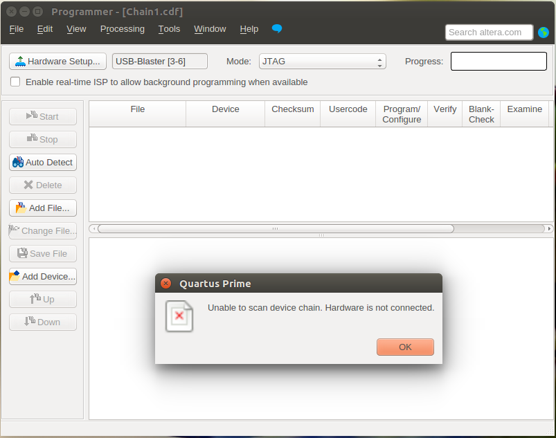
The PIC board, MAX10-JB,should work as a USB-Blaster download cable, but it seems that something is wrong somewhere.
% dmesg
[   99.874756] usb 3-6: new full-speed USB device number 5 using xhci_hcd
[  100.005217] usb 3-6: New USB device found, idVendor=09fb, idProduct=6001
[  100.005224] usb 3-6: New USB device strings: Mfr=1, Product=2, SerialNumber=3
[  100.005229] usb 3-6: Product: USB-Blaster
[  100.005232] usb 3-6: Manufacturer: Altera

% lsusb
Bus 003 Device 005: ID 09fb:6001 Altera Blaster

% sudo ./jtagd --foreground --debug
JTAG daemon started
Using config file /etc/jtagd/jtagd.conf
Remote JTAG permitted when password set
USB-Blaster added "USB-Blaster [3-6]"

USB-Blaster port (/dev/bus/usb/003/005) opened
USB-Blaster port (/dev/bus/usb/003/005) opened

% ls -l /dev/bus/usb/003/005
crw-rw-rw- 1 root root 189, 260 May 18 16:30 /dev/bus/usb/003/005

% cat /etc/udev/rules.d/51-usbblaster.rules
# Altera USB-Blaster for Quartus FPGA Software
SUBSYSTEMS=="usb", ATTR{idVendor}=="09fb", ATTR{idProduct}=="6001", MODE="0666"
SUBSYSTEMS=="usb", ATTR{idVendor}=="09fb", ATTR{idProduct}=="6002", MODE="0666"
SUBSYSTEMS=="usb", ATTR{idVendor}=="09fb", ATTR{idProduct}=="6003", MODE="0666"

This is something I felt uneasy in FPGA CW Keyer (4) when I added dot and dash memories.

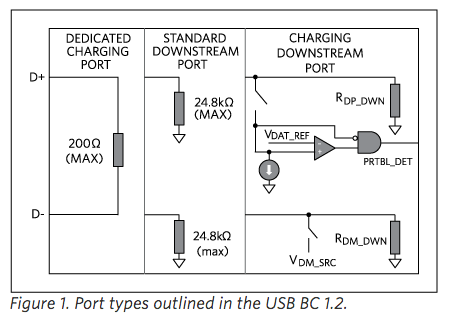
Receiving DC power (+5V) via USB I/F is somewhat complicated due to various standard and custom protocols employed. Sometimes D+ and D- lines are used to convey information.
https://www.maximintegrated.com/en/app-notes/index.mvp/id/5801
http://www.ti.com/lit/ds/symlink/tps2540a.pdf
This causes a problem with the PIC board, MAX10-JB, because some of the I/O pins of the PIC microcontroller are used both for D+ and D- lines for USB I/F, and for writing into its flash program memory.
To avoid interference, I pulled off the USB cable and used an external power supply just while programming the flash memory.
The green flushing LED on the FPGA evaluation board, MAX10-FB, shows that the flash memory was successfully programmed and the verification was OK.
Here is an HDL design example given by Altera.
// 4-State Moore state machine

// A Moore machine's outputs are dependent only on the current state.
// The output is written only when the state changes.  (State
// transitions are synchronous.)

module moore_mac
(
	input	clk, data_in, reset,
	output reg [1:0] data_out
);

	// Declare state register
	reg		[1:0]state;

	// Declare states
	parameter S0 = 0, S1 = 1, S2 = 2, S3 = 3;

	// Output depends only on the state
	always @ (state) begin
		case (state)
			S0:
				data_out = 2'b01;
			S1:
				data_out = 2'b10;
			S2:
				data_out = 2'b11;
			S3:
				data_out = 2'b00;
			default:
				data_out = 2'b00;
		endcase
	end

	// Determine the next state
	always @ (posedge clk or posedge reset) begin
		if (reset)
			state <= S0;
		else
			case (state)
				S0:
					state <= S1;
				S1:
					if (data_in)
						state <= S2;
					else
						state <= S1;
				S2:
					if (data_in)
						state <= S3;
					else
						state <= S1;
				S3:
					if (data_in)
						state <= S2;
					else
						state <= S3;
			endcase
	end

endmodule
You can copy and paste such example codes, or can insert the code from a template if you are using Quartus Prime.
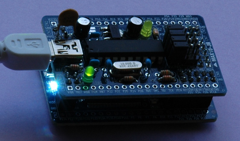
A PIC board, MAX10-JB, is plugged on top of the FPGA evaluation board, MAX10-FB. A bright white LED is flushing to indicate that the pre-mounted FPGA is working fine with a pre-programmed configuration.
The PIC board works like an Altera’s USB-Blaster Download Cable.

https://www.altera.com/en_US/pdfs/literature/hb/qts/qts-qps-handbook.pdf
There are recommended practices in almost everything.
For example, The ARRL Operating Manual says that “When replying to a CQ, give both call signs clearly — yours and the CQing station.”
So I am now learning recommended design practices and coding styles for FPGAs. Of course, the practices differ a lot depending on the devices you use and the development tools employed.
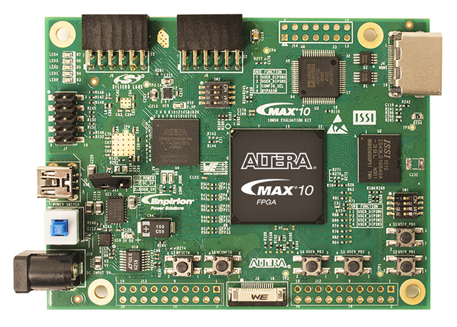
Various kinds of evaluation kits are available. This board is from Altera and looks very nice with on-board HDMI output capability.
https://www.altera.com/products/boards_and_kits/dev-kits/altera/kit-max-10m50-evaluation.html
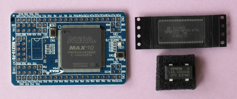
Here is the board I am going to use. An FPGA, Altera’s MAX 10 (10M08SAE144C8G), is pre-mounted, but you need to solder other parts, such as a 256kbit SDRAM, and a 48MHz Xtal oscillator.
More detailed description of the board is here.
(No, I don’t think they have pages written in English.)

It might be easier to use a state transition table to realize squeeze operations.
//------- ELK Test Bench ---------
`timescale 1ms/1us

module tb_elk;

    reg RST_N;
    reg CLK;
    reg IN_DOT;
    reg IN_DASH;

ELK ELK_0(.RST_N   (RST_N),
          .CLK     (CLK)  ,
          .IN_DOT  (IN_DOT)  ,
          .IN_DASH (IN_DASH)  ,
          .KEY_OUT (KEY_OUT)   );

initial begin
    CLK <= 1'b1;
    forever begin
        #10;
        CLK <= ~CLK;
    end
end

initial begin
    RST_N <= 1'b0;
     #50;
    RST_N <= 1'b1;
    #1100000;
    $finish;
end

initial begin
    IN_DOT <= 1'b1; #063;
    IN_DOT <= 1'b0; #073;
    IN_DOT <= 1'b1; #323;
    IN_DOT <= 1'b0; #223;
    IN_DOT <= 1'b1; #243;
    IN_DOT <= 1'b0; #023;
    IN_DOT <= 1'b1; #1000000;
end

initial begin
    IN_DASH <= 1'b1; #183;
    IN_DASH <= 1'b0; #123;
    IN_DASH <= 1'b1; #223;
    IN_DASH <= 1'b0; #023;
    IN_DASH <= 1'b1; #260;
    IN_DASH <= 1'b0; #300;
    IN_DASH <= 1'b1; #1000000;
end

endmodule
module ELK(RST_N, CLK, IN_DOT, IN_DASH, KEY_OUT);

    input RST_N;
    input CLK;
    input IN_DOT;
    input IN_DASH;
    output KEY_OUT;

    reg      KEY_OUT;
    reg      m_dot;
    reg      m_dash;
    reg[2:0] r_state;

//--------- dot memory ---------------------
    always @ (negedge IN_DOT or negedge RST_N) begin
        if ( RST_N == 1'b0 ) begin
            m_dot  <= 1'b0;
        end if ( IN_DOT == 1'b0) begin
            m_dot  <= 1'b1;
        end
    end

//--------- dash memory ---------------------
    always @ (negedge IN_DASH or negedge RST_N) begin
        if ( RST_N == 1'b0 ) begin
            m_dash  <= 1'b0;
        end if ( IN_DASH == 1'b0) begin
            m_dash  <= 1'b1;
        end
    end

//--------- state output ---------------------
    always @ (r_state) begin
        case(r_state)
            3'b000: begin KEY_OUT <= 1'b0; end
            3'b001: begin KEY_OUT <= 1'b1; end
            3'b010: begin KEY_OUT <= 1'b1; end
            3'b011: begin KEY_OUT <= 1'b1; end
            3'b100: begin KEY_OUT <= 1'b0; end
            3'b101: begin KEY_OUT <= 1'b1; end
            3'b110: begin KEY_OUT <= 1'b0; end
        default:begin
        end
        endcase
    end

//--------- state transition ---------------------
    always @ (posedge CLK or negedge RST_N) begin
        if ( RST_N == 1'b0 ) begin
            r_state <= 3'b000;
        end else
        case (r_state)
        3'b000:begin // idle
            if(IN_DASH == 1'b0) begin
                r_state <= 3'b001;
            end else if(IN_DOT == 1'b0) begin
                r_state <= 3'b101;
            end
        end
        3'b001:begin // dash running 1
                r_state <= 3'b010;
                m_dash  <= 1'b0;
        end
        3'b010:begin // dash running 2
                r_state <= 3'b011;
        end
        3'b011:begin // dash running 3
                r_state <= 3'b100;
        end
        3'b100:begin // dash running 4
            if(IN_DOT == 1'b0 || m_dot == 1'b1) begin
                r_state <= 3'b101;
                m_dot   <= 1'b0;
            end else if(IN_DASH == 1'b0) begin
                r_state <= 3'b001;
            end else begin
                r_state <= 3'b000;
            end
        end
        3'b101:begin // dot running 1
                r_state <= 3'b110;
                m_dot   <= 1'b0;
        end
        3'b110:begin // dot running 2
            if(IN_DASH == 1'b0 || m_dash == 1'b1) begin
                r_state <= 3'b001;
                m_dash  <= 1'b0;
            end else if(IN_DOT == 1'b0) begin
                r_state <= 3'b101;
            end else begin
                r_state <= 3'b000;
            end
        end
        default:begin
        end
        endcase
    end

endmodule
Now, DASHes only.
    reg[1:0] r_dash;
    wire     w_dash;

//---------- generate dash ---------------------
    always @ ( posedge CLK or negedge RST_N) begin
        if ( RST_N == 1'b0 ) begin
            r_dash <= 2'h0;
        end
        else if ( IN_DASH == 1'b0 || r_dash != 2'h0 ) begin
            if ( r_dash == 2'h3 ) begin
                r_dash <= 2'h0;
            end
            else begin
                r_dash <= r_dash + 2'h1;
            end
        end
        else begin
            r_dash <= 2'h0;
        end
    end

//---------- w_dash ----------------------------

    assign w_dash = ( r_dash == 2'h0 ) ? 1'b0 : 1'b1;